STM32 Power saving: STM32F4 black-pill manages clock and frequencies – 2
An essential factor of our micro-controllers is power consumption. As usual, I started to analyze that aspect without entering the detail for sleep mode but with some alternative solutions offered by the microcontroller.
The frequency scaling in the STM32 is more complex than in other microcontrollers, in particular, because the architecture is more complex, and STM32 chose to give the instrument to simplify that management and not to masquerade the complexity.
Here my selection of STM32 STM32F103C8T6 STM32F401 STM32F411 ST-Link v2 ST-Link v2 official
Here my tested multimeters Aneng SZ18
So the first thing to do to approach that argument is to download the STM32CubeIDE because, even if you don’t develop with the native interpreter of STM32, the Arduino core wraps the function of the native core (this generates a higher space in Flash memory), and grant the possibility to use some code generator.
STM32CubeIDE
STM32CubeIDE is an all-in-one multi-OS development tool that is part of the STM32Cube software ecosystem. STM32CubeIde is a C/C++ development platform with peripheral configuration, code generation, code compilation, and debug features for STM32 microcontrollers and microprocessors.
You can download It from this link.
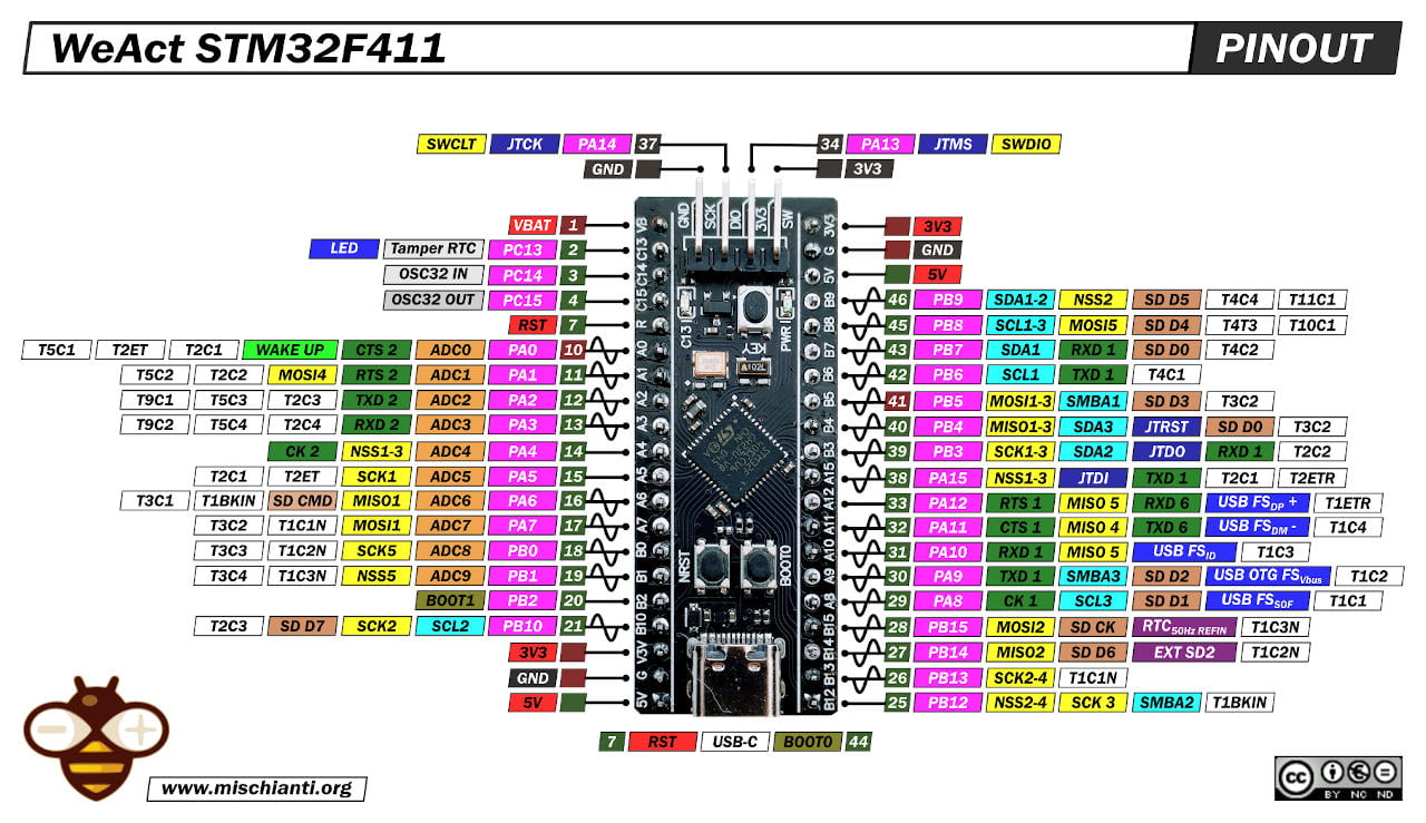
Configure STM32F4 black-pill
This IDE allows you to program the native STM32 chip, but we don’t use the chip directly, so we need to recreate the prototyping board.
For example, the chip-like STM32F4 doesn’t have an external oscillator (LSE and HSE), but the STM32F411CEU6 black pill prototyping board have these peripherals integrated.
You can check the schema in the detailed article about STM32F411CEU6.
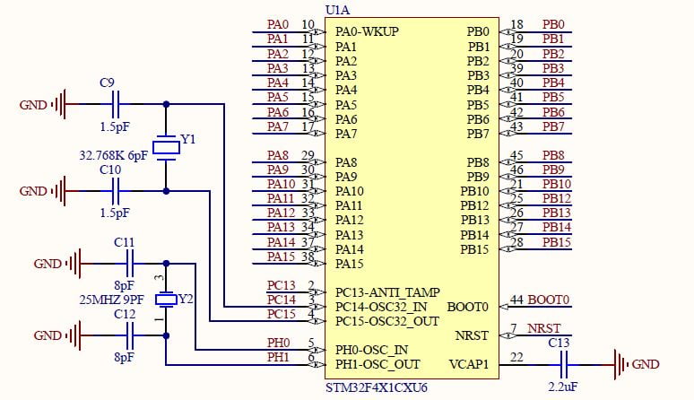
To simplify your work, I share a project file with all configured as expected: STM32F411 black pill.
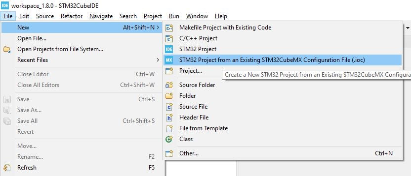
Load the project by using File --> New --> STM32 Project from Existing STM32CubeMX Configuration File (.ioc)
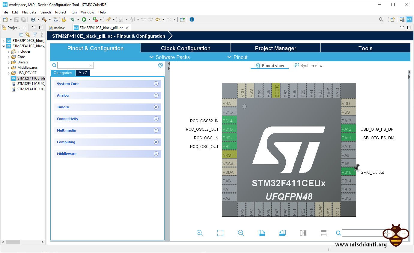
Now you have a project completely initialized but empty. You can do double click on .ioc file, and you land on the Pinout & Configuration the tab of the configurator.
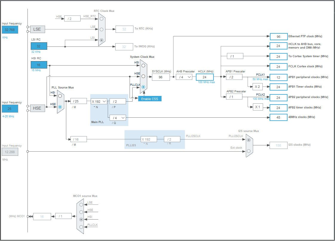
You can retrieve the clock’s complete editable block/flow diagram when you click on the clock configuration.
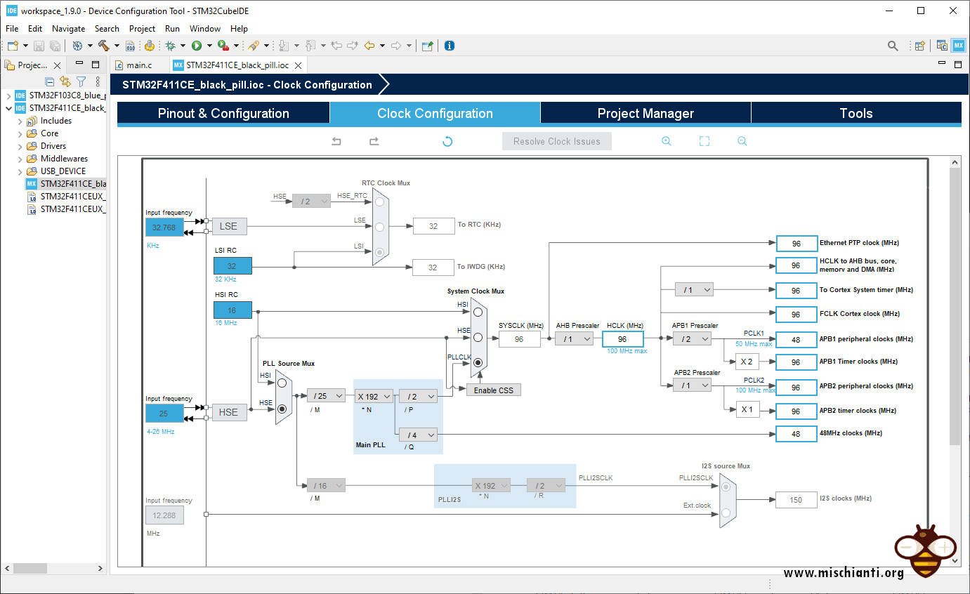
The diagram shows four clocks, two internal LSI and HSI, and two external HSE and LSE.
But before analyzing that diagram, we are looking at the basic architecture of an STM32.
STM32F4 Architecture
To help understand the architecture, we use a block diagram.
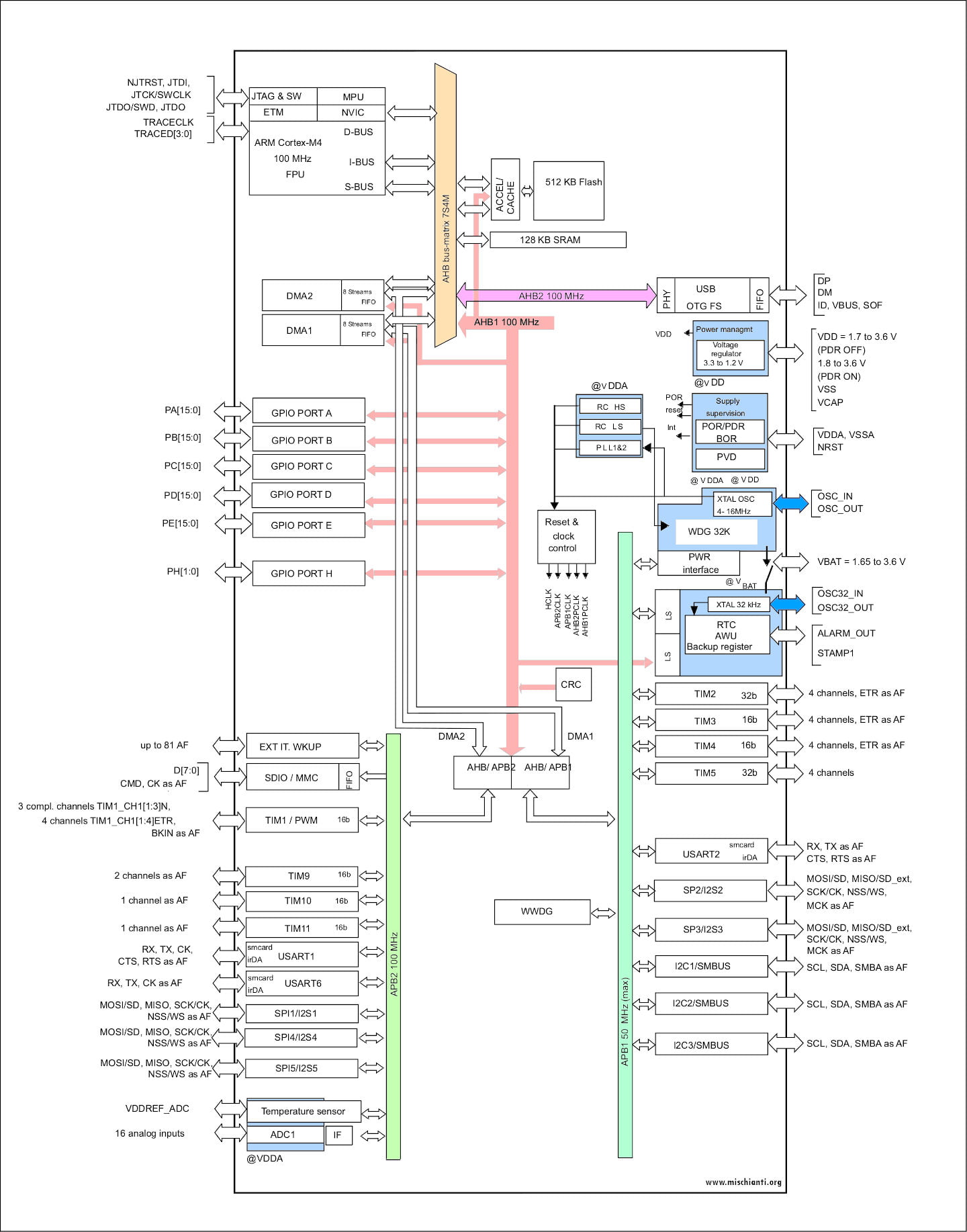
Some central parts aren’t used in this tutorial, and I describe them here.
- DMA (Direct Memory Access, Direct memory access) allows hardware devices of different speeds to communicate; it doesn’t have to depend on the CPU’s Large amount of interrupt load.
- SRAM(Static Random-Access Memory, Static random access memory) So-called “ static state ” means that this kind of memory, as long as it remains powered on, The data stored in it can be kept constant;
- FSMC (Flexible Static Memory Controller, Variable static storage controller ), Ability to work with synchronous or asynchronous storage and 16 position PC Memory card connection, STM32 Of FSMC Interface support includes SRAM, NAND FLASH, NOR FLASH, and PSRAM Equal storage.
- DRAM(Dynamic Random Access Memory, Dynamic random access memory) The data stored in it needs to be updated periodically.
However, When the power supply stops, SRAM The stored data will still disappear (go by the name of volatile memory); it’s the same as being able to store data after a power failure ROM Or flash memory FLASH Is different. - I-Bus: take M4, The instruction bus of the kernel and FLASH Command interface connection, Used for Instruction prefetching.
D-Bus: take M4 Kernel data bus and FLASH Data interface connection, constant loading, and debugging.
The remaining parts are what we need, and all the peripherals are managed with two bus APBx; naturally, these buses are synchronized with clocks and are used to manage all. And now we can go in deep on clock configuration.
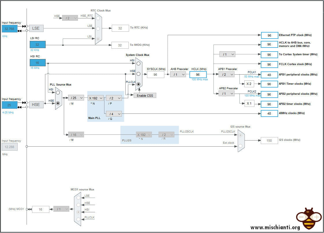
Clocks diagram
As already described, we can examine four clocks’ sources.
- High-speed external clock (HSE): The external crystal oscillator is used as the clock source, and the crystal oscillator frequency is in the range of 4 to 26 MHz, and the crystal oscillator of 25 MHz is generally used.
- High-Speed Internal Clock (HSI): Generated by the internal RC oscillator with a frequency of 16 MHz, but not stable, and the accuracy is not high.
- Low-speed external clock (LSE): The external crystal oscillator is used as the clock source, which is mainly provided to the real-time clock module, so 32.768 kHz is generally used.
- Low-speed internal clock (LSI): Generated by the internal RC oscillator, also mainly supplied to the real-time clock module, with a frequency of approximately 32kHz, provides a low-power clock.
Now we can add the block diagram of STM32CubeIde with the default STM32F411 black-pill configuration again.
With this diagram, we can follow the flow of the clock starting from PLL Source Mux.
PLL clock source
There are two PLL clock sources: one is HSE, the other is HSI, and one is HSI which is the internal high-speed clock signal with a frequency of 16MHz. The frequency will drift according to temperature and environmental conditions. Generally, it is not used as the clock source of PLL, so HSE is selected as the clock source of PLL.
Main PLL
This device has a main divider from 2 to 63 before the Main PLL then a big multiplication factor of the PLL from 50 to 432 can be applied. But a better solution than STM32F1 is the separated dividers one for AHB and one only for the USB. So the HSE of 25MHz are divided to 25 then multiplied from 192 and divided for 2 for the main bug and for 4 for the USB, an efficient solution respect other devices. SYSCLK = 25MHz / 25 * 192 /2 = 96MHz.
Clock Security System (CSS)
If the HSE clock fails, the HSE oscillator is automatically shut down, and the clock failure event will be sent to the brake input of the advanced timers (TIM1 and TIM8), and a clock safety interrupts CSSI will be generated, allowing the software to complete the rescue operation. This CSSI interrupt is connected to the NMI interrupt (non-maskable interrupt) of Cortex™-M3.
USB Clock
There is a full-speed USB module in STM32, and its serial interface engine requires a clock source with a frequency of 48MHz. The clock source can only be obtained from the output of the PLL (the only one). It can be divided from 2 to 48.
System Clock Mux SYSCLK
The system clock source can be HSI, PLLCLK, and HSE. Set the system clock here: SYSCLK=PLLCLK=96MHz.
AHB bus clock HCLK
The clock obtained after the system clock SYSCLK is divided by the AHB Prescaler is called the APB bus clock, that is, HCLK, and this is delivered to AHB bus, core, memory, flash, and DMA. The frequency division factor can be [1, 2, 4, 8, 16, 64, 128, 256, 512]. The clocks of most of the peripherals on the chip are obtained by HCLK frequency division. As for the clock setting of the peripherals on the AHB bus, it must be set when the peripherals are used. Here, you only need to roughly set the APB clocks it is set to divide by 1, that is, HCLK=SYSCLK/1_AHB=96MHz.
APB2 bus clock PCLK2
The APB2 (High-speed peripherals) bus clock PCLK2 (Peripheral clock) is obtained by HCLK through the high-speed APB2 Prescaler, and the frequency division factor can be [1, 2, 4, 8, 16]. HCLK2 is a high-speed bus clock, and on-chip high-speed peripherals are mounted on this bus, such as all GPIO, USART1, SPI1, etc. As for the clock setting of the peripheral on the APB2 bus, it must be set when the peripheral is used. Here, it is only necessary to set the clock of APB2 roughly and set it to 1 frequency division, that is, PCLK2=HCLK=96MHz.
APB1 bus clock PCLK1
The APB1 (Low-speed peripherals) bus clock PCLK1 (Peripheral clock) is obtained by HCLK through the low-speed APB Prescaler, and the frequency division factor can be [1, 2, 4, 8, 16]. HCLK1 is a low-speed bus clock, up to 36MHz; on-chip low-speed peripherals are mounted on this bus, such as USART 2/3/4/5, SPI 2/3, I2C 1/2, etc. As for the clock setting of the peripheral on the APB1 bus, it has to wait until the peripheral is used. Here, you only need to set the clock of APB1 roughly and set it to divide by 2, that is, PCLK1=HCLK/2=48MHz.
Other
Cortex system clock
The Cortex system clock is obtained by dividing HCLK by 8, which is equal to 12MHz. The Cortex system clock is used to drive the system timer SysTick of the kernel. SysTick is generally used for the clock beat of the operating system and can also be used for ordinary timing.
RTC clock, independent watchdog clock
The RTC clock can be obtained by dividing the frequency of HSE/128, or the low-speed external clock signal LSE can provide it with a frequency of 32.768kHz, or it can be provided by the low-speed internal clock signal HSI. The clock of the independent watchdog is provided by LSI and can only be provided by LSI. LSI is a low-speed internal clock signal with a frequency of 30-60kHz, generally 32kHz.
MCO clock output
MCO is the abbreviation of Microcontroller Clock Output. It is the clock output pin of the microcontroller. PA8 multiplexes it in the STM32 F1 series. Its primary function is to provide a clock to the outside world, which is equivalent to an active crystal oscillator. In addition to giving a clock to the outside world, we can also monitor the clock output of the MCO pin with an oscilloscope to verify that the system clock configuration is correct. The clock source of the MCO can be PLLCLK/2, HSI, HSE, and SYSCLK.
Change clock configuration
Now we know how STM32 is composed, and we can try to change that values according to the previous schema to save power.
To change that parameter STM32 core gives us the possibility to override the default value in practice; the declaration of the function in the core is marked WAKE, and so you override It with the use of extern.
WEAK void SystemClock_Config(void)
{
[...]
}
To do a full test for many situations, I use ST-LINK and external FDTI for debugging; I’d like to use Serial2 because USART2 works on APB2 and uses the low-speed buffer.
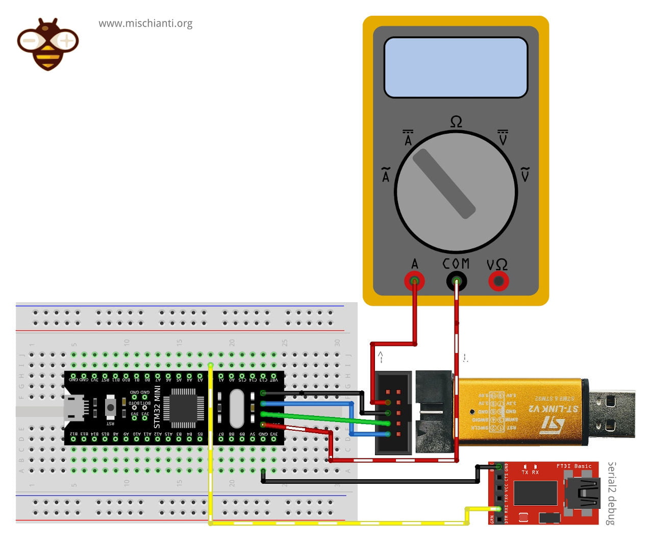
But I think you can use the standard without a problem Serial.
But pay attention, you can’t use USB Serial debug because we will put the USB out of order with the frequency management.
Get current frequences
Now we are going to launch a simple sketch, and we will use a series of prints to show current frequences.
/**
 * Test SysClock configuration on STM32
 * Disable USB Serial2
 * and use an external
 *
 * by Renzo Mischianti <www.mischianti.org>
 */

// If you use generic STM32F411CE
// you don't need this explicit declaration
// This is needed by blackpill specified version
HardwareSerial Serial2(USART2);   // PA3  (RX)  PA2  (TX)

void setup() {
  Serial2.begin(115200);
  while (!Serial2){ delay(100); }
  Serial2.println("START!");
}

void loop() {
  Serial2.println("------------------------------------");
  Serial2.printf("SYCLK= %dMHz\n", HAL_RCC_GetSysClockFreq()/1000000);

  Serial2.printf("HCLK = %dMHz\n", HAL_RCC_GetHCLKFreq()/1000000);
  Serial2.printf("APB1 = %dMHz\n", HAL_RCC_GetPCLK1Freq()/1000000);
  Serial2.printf("APB2 = %dMHz\n", HAL_RCC_GetPCLK2Freq()/1000000);
  Serial2.println("------------------------------------");
  Serial2.println();
  delay(5000);
}
As expected, the result.
------------------------------------
SYCLK= 96MHz
HCLK = 96MHz
APB1 = 48MHz
APB2 = 96MHz
------------------------------------
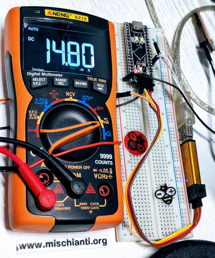
We can see in the multimeter a power consumption of 31,20mAh.
Now we try to create a configuration that replicates standard settings, I add here the whole sketch, and now we are going to do the verification.
/**
 * Test SysClock configuration on STM32
 * Disable USB Serial2
 * and use an external
 *
 * by Renzo Mischianti <www.mischianti.org>
 */

// If you use generic STM32F411CE
// you don't need this explicit declaration
// This is needed by blackpill specified version
HardwareSerial Serial2(USART2);   // PA3  (RX)  PA2  (TX)

/**
  * Standard configuration
  *  @brief  System Clock Configuration
  *         The system Clock is configured as follow :
  *            System Clock source            = PLL (HSE)
  *            SYSCLK(Hz)                     = 96000000
  *            HCLK(Hz)                       = 96000000
  *            AHB Prescaler                  = 1
  *            APB1 Prescaler                 = 2
  *            APB2 Prescaler                 = 1
  *            PLL_Source                     = HSE
  *            PLL_M_Prescaler                = 25
  *            PLL_N_Mux                      = 192
  *            PLL_P_Prescaler                = 2
  *            PLL_Q_Prescaler                = 4
  *            Flash Latency(WS)              = 3
  * @param  None
  * @retval None
  */
extern "C" void SystemClock_Config(void)
{
  RCC_OscInitTypeDef RCC_OscInitStruct = {0};
  RCC_ClkInitTypeDef RCC_ClkInitStruct = {0};

  /** Configure the main internal regulator output voltage
  */
  __HAL_RCC_PWR_CLK_ENABLE();
  __HAL_PWR_VOLTAGESCALING_CONFIG(PWR_REGULATOR_VOLTAGE_SCALE1);

  /** Initializes the RCC Oscillators according to the specified parameters
  * in the RCC_OscInitTypeDef structure.
  */
  RCC_OscInitStruct.OscillatorType = RCC_OSCILLATORTYPE_HSE;
  RCC_OscInitStruct.HSEState = RCC_HSE_ON;
  RCC_OscInitStruct.PLL.PLLState = RCC_PLL_ON;
  RCC_OscInitStruct.PLL.PLLSource = RCC_PLLSOURCE_HSE;
  RCC_OscInitStruct.PLL.PLLM = 25;
  RCC_OscInitStruct.PLL.PLLN = 192;
  RCC_OscInitStruct.PLL.PLLP = RCC_PLLP_DIV2;
  RCC_OscInitStruct.PLL.PLLQ = 4;
  if (HAL_RCC_OscConfig(&RCC_OscInitStruct) != HAL_OK)
  {
    Error_Handler();
  }

  /** Initializes the CPU, AHB and APB buses clocks
  */
  RCC_ClkInitStruct.ClockType = RCC_CLOCKTYPE_HCLK|RCC_CLOCKTYPE_SYSCLK
                              |RCC_CLOCKTYPE_PCLK1|RCC_CLOCKTYPE_PCLK2;
  RCC_ClkInitStruct.SYSCLKSource = RCC_SYSCLKSOURCE_PLLCLK;
  RCC_ClkInitStruct.AHBCLKDivider = RCC_SYSCLK_DIV1;
  RCC_ClkInitStruct.APB1CLKDivider = RCC_HCLK_DIV2;
  RCC_ClkInitStruct.APB2CLKDivider = RCC_HCLK_DIV1;

  if (HAL_RCC_ClockConfig(&RCC_ClkInitStruct, FLASH_LATENCY_3) != HAL_OK)
  {
    Error_Handler();
  }
}

void setup() {
  Serial2.begin(115200);
  while (!Serial2){ delay(100); }
  Serial2.println("START!");
}

void loop() {
  Serial2.println("------------------------------------");
  Serial2.printf("SYCLK= %dMHz\n", HAL_RCC_GetSysClockFreq()/1000000);

  Serial2.printf("HCLK = %dMHz\n", HAL_RCC_GetHCLKFreq()/1000000);
  Serial2.printf("APB1 = %dMHz\n", HAL_RCC_GetPCLK1Freq()/1000000);
  Serial2.printf("APB2 = %dMHz\n", HAL_RCC_GetPCLK2Freq()/1000000);
  Serial2.println("------------------------------------");
  Serial2.println();
  delay(5000);
}
And the output result is the same:
------------------------------------
SYCLK= 96MHz
HCLK = 96MHz
APB1 = 48MHz
APB2 = 96MHz
------------------------------------
Some minor change on power consumption (probably we change divider respect to the original) now is 31.50mAh.
First frequencies reduction test
Now we are going to make a little reduction of the frequencies, and we are going to check the result.
As you can see in the block diagram, we make a good reduction of AHB Prescaler with the consequential reduction of HCLK frequencies with the consequent decrease in the peripheral.
/**
 * Test SysClock configuration on STM32
 * Disable USB Serial2
 * and use an external
 *
 * by Renzo Mischianti <www.mischianti.org>
 */

// If you use generic STM32F411CE
// you don't need this explicit declaration
// This is needed by blackpill specified version
HardwareSerial Serial2(USART2);   // PA3  (RX)  PA2  (TX)

/**
  * First try reduction
  *  @brief  System Clock Configuration
  *         The system Clock is configured as follow :
  *            System Clock source            = PLL (HSE)
  *            SYSCLK(Hz)                     = 96000000
  *            HCLK(Hz)                       = 96000000  --> 24000000
  *            AHB Prescaler                  = 1         --> 4
  *            APB1 Prescaler                 = 2
  *            APB2 Prescaler                 = 1
  *            PLL_Source                     = HSE
  *            PLL_M_Prescaler                = 25
  *            PLL_N_Mux                      = 192
  *            PLL_P_Prescaler                = 2
  *            PLL_Q_Prescaler                = 4
  *            Flash Latency(WS)              = 3
  * @param  None
  * @retval None
  */
extern "C" void SystemClock_Config(void)
{
  RCC_OscInitTypeDef RCC_OscInitStruct = {0};
  RCC_ClkInitTypeDef RCC_ClkInitStruct = {0};

  /** Configure the main internal regulator output voltage
  */
  __HAL_RCC_PWR_CLK_ENABLE();
  __HAL_PWR_VOLTAGESCALING_CONFIG(PWR_REGULATOR_VOLTAGE_SCALE1);

  /** Initializes the RCC Oscillators according to the specified parameters
  * in the RCC_OscInitTypeDef structure.
  */
  RCC_OscInitStruct.OscillatorType = RCC_OSCILLATORTYPE_HSE;
  RCC_OscInitStruct.HSEState = RCC_HSE_ON;
  RCC_OscInitStruct.PLL.PLLState = RCC_PLL_ON;
  RCC_OscInitStruct.PLL.PLLSource = RCC_PLLSOURCE_HSE;
  RCC_OscInitStruct.PLL.PLLM = 25;
  RCC_OscInitStruct.PLL.PLLN = 192;
  RCC_OscInitStruct.PLL.PLLP = RCC_PLLP_DIV2;
  RCC_OscInitStruct.PLL.PLLQ = 4;
  if (HAL_RCC_OscConfig(&RCC_OscInitStruct) != HAL_OK)
  {
    Error_Handler();
  }

  /** Initializes the CPU, AHB and APB buses clocks
  */
  RCC_ClkInitStruct.ClockType = RCC_CLOCKTYPE_HCLK|RCC_CLOCKTYPE_SYSCLK
                              |RCC_CLOCKTYPE_PCLK1|RCC_CLOCKTYPE_PCLK2;
  RCC_ClkInitStruct.SYSCLKSource = RCC_SYSCLKSOURCE_PLLCLK;
  RCC_ClkInitStruct.AHBCLKDivider = RCC_SYSCLK_DIV4;
  RCC_ClkInitStruct.APB1CLKDivider = RCC_HCLK_DIV2;
  RCC_ClkInitStruct.APB2CLKDivider = RCC_HCLK_DIV1;

  if (HAL_RCC_ClockConfig(&RCC_ClkInitStruct, FLASH_LATENCY_3) != HAL_OK)
  {
    Error_Handler();
  }
}

void setup() {
  Serial2.begin(115200);
  while (!Serial2){ delay(100); }
  Serial2.println("START!");
}

void loop() {
  Serial2.println("------------------------------------");
  Serial2.printf("SYCLK= %dMHz\n", HAL_RCC_GetSysClockFreq()/1000000);

  Serial2.printf("HCLK = %dMHz\n", HAL_RCC_GetHCLKFreq()/1000000);
  Serial2.printf("APB1 = %dMHz\n", HAL_RCC_GetPCLK1Freq()/1000000);
  Serial2.printf("APB2 = %dMHz\n", HAL_RCC_GetPCLK2Freq()/1000000);
  Serial2.println("------------------------------------");
  Serial2.println();
  delay(5000);
}
The console output now is
------------------------------------
SYCLK= 96MHz
HCLK = 24MHz
APB1 = 12MHz
APB2 = 24MHz
------------------------------------
And we have a good reduction of mAh, and the multimeter result is 14.65mAh.
Better reduction of frequencies
Now we will reduce some frequencies without putting out of order any peripheral to maintain the exact behavior of a sketch.

In this case, we are going to touch Main PLL with the reduction of multiplex and some adjustments to don’t put out-of-order the USB.
/**
 * Test SysClock configuration on STM32
 * Disable USB Serial2
 * and use an external
 *
 * by Renzo Mischianti <www.mischianti.org>
 */

// If you use generic STM32F411CE
// you don't need this explicit declaration
// This is needed by blackpill specified version
HardwareSerial Serial2(USART2);   // PA3  (RX)  PA2  (TX)

/**
  * First test reduction
  *  @brief  System Clock Configuration
  *         The system Clock is configured as follow :
  *            System Clock source            = PLL (HSE)
  *            SYSCLK(Hz)                     = 96000000  --> 36000000
  *            HCLK(Hz)                       = 96000000  --> 36000000
  *            AHB Prescaler                  = 1
  *            APB1 Prescaler                 = 2
  *            APB2 Prescaler                 = 1
  *            PLL_Source                     = HSE
  *            PLL_M_Prescaler                = 25
  *            PLL_N_Mux                      = 192       --> 144
  *            PLL_P_Prescaler                = 2         --> 4
  *            PLL_Q_Prescaler                = 4         --> 3
  *            Flash Latency(WS)              = 1
  * @param  None
  * @retval None
  */
extern "C" void SystemClock_Config(void)
{
  RCC_OscInitTypeDef RCC_OscInitStruct = {0};
  RCC_ClkInitTypeDef RCC_ClkInitStruct = {0};

  /** Configure the main internal regulator output voltage
  */
  __HAL_RCC_PWR_CLK_ENABLE();
  __HAL_PWR_VOLTAGESCALING_CONFIG(PWR_REGULATOR_VOLTAGE_SCALE1);

  /** Initializes the RCC Oscillators according to the specified parameters
  * in the RCC_OscInitTypeDef structure.
  */
  RCC_OscInitStruct.OscillatorType = RCC_OSCILLATORTYPE_HSE;
  RCC_OscInitStruct.HSEState = RCC_HSE_ON;
  RCC_OscInitStruct.PLL.PLLState = RCC_PLL_ON;
  RCC_OscInitStruct.PLL.PLLSource = RCC_PLLSOURCE_HSE;
  RCC_OscInitStruct.PLL.PLLM = 25;
  RCC_OscInitStruct.PLL.PLLN = 144;
  RCC_OscInitStruct.PLL.PLLP = RCC_PLLP_DIV4;
  RCC_OscInitStruct.PLL.PLLQ = 3;
  if (HAL_RCC_OscConfig(&RCC_OscInitStruct) != HAL_OK)
  {
    Error_Handler();
  }

  /** Initializes the CPU, AHB and APB buses clocks
  */
  RCC_ClkInitStruct.ClockType = RCC_CLOCKTYPE_HCLK|RCC_CLOCKTYPE_SYSCLK
                              |RCC_CLOCKTYPE_PCLK1|RCC_CLOCKTYPE_PCLK2;
  RCC_ClkInitStruct.SYSCLKSource = RCC_SYSCLKSOURCE_PLLCLK;
  RCC_ClkInitStruct.AHBCLKDivider = RCC_SYSCLK_DIV1;
  RCC_ClkInitStruct.APB1CLKDivider = RCC_HCLK_DIV2;
  RCC_ClkInitStruct.APB2CLKDivider = RCC_HCLK_DIV1;

  if (HAL_RCC_ClockConfig(&RCC_ClkInitStruct, FLASH_LATENCY_1) != HAL_OK)
  {
    Error_Handler();
  }
}


void setup() {
  Serial2.begin(115200);
  while (!Serial2){ delay(100); }
  Serial2.println("START!");
}

void loop() {
  Serial2.println("------------------------------------");
  Serial2.printf("SYCLK= %dMHz\n", HAL_RCC_GetSysClockFreq()/1000000);

  Serial2.printf("HCLK = %dMHz\n", HAL_RCC_GetHCLKFreq()/1000000);
  Serial2.printf("APB1 = %dMHz\n", HAL_RCC_GetPCLK1Freq()/1000000);
  Serial2.printf("APB2 = %dMHz\n", HAL_RCC_GetPCLK2Freq()/1000000);
  Serial2.println("------------------------------------");
  Serial2.println();
  delay(5000);
}
And here is the console output result
------------------------------------
SYCLK= 36MHz
HCLK = 36MHz
APB1 = 18MHz
APB2 = 36MHz
------------------------------------
As expected, we have an outstanding reduction of the power consumption, but remember all performance of our STM32 is reduced.
In this configuration, we have 10.90mAh.
Conclusion
We noticed that the possibility of STM32 is a lot, and we must know the architecture very well if we want to get better results. We can consider to lost some peripheral if not needed and adding more power to some specified functional unit.
Thanks
- STM32F1 Blue-Pill: pinout, specs, and Arduino IDE configuration (STM32duino and STMicroelectronics)
- STM32: program (STM32F1) via USB with STM32duino bootloader
- STM32: programming (STM32F1 STM32F4) via USB with HID boot-loader
- STM32F4 Black-Pill: pinout, specs, and Arduino IDE configuration
- STM32: ethernet w5500 with plain HTTP and SSL (HTTPS)
- STM32: ethernet enc28j60 with plain HTTP and SSL (HTTPS)
- STM32: WiFiNINA with ESP32 WiFi Co-Processor
- How to use SD card with stm32 and SdFat library
- \STM32: SPI flash memory FAT FS
- STM32: internal RTC, clock, and battery backup (VBAT)
- STM32 LoRa
- STM32 Power saving
- STM32F1 Blue-Pill clock and frequency management
- STM32F4 Black-Pill clock and frequency management
- Intro and Arduino vs STM framework
- Library LowPower, wiring, and Idle (STM Sleep) mode
- Sleep, deep sleep, shutdown, and power consumption
- Wake up from RTC alarm and Serial
- Wake up from the external source
- Backup domain intro and variable preservation across reset
- RTC backup register and SRAM preservation
- STM32 send emails with attachments and SSL (like Gmail): w5500, enc28j60, SD, and SPI Fash
- FTP server on STM32 with w5500, enc28j60, SD Card, and SPI Flash